- 您现在的位置:买卖IC网 > Sheet目录2006 > LTC2495CUHF#PBF (Linear Technology)IC ADC 16BIT W/PGA 38-QFN
LTC2495
0
2495fd
Rejection Mode (FA, FB)
The LTC2495 includes a high accuracy on-chip oscillator
with no required external components. Coupled with an
integrated fourth-order digital lowpass filter, the LTC2495
rejects line frequency noise. In the default mode, the
LTC2495 simultaneously rejects 50Hz and 60Hz by at least
87dB. If more rejection is required, the LTC2495 can be
configured to reject 50Hz or 60Hz to better than 110dB.
Speed Mode (SPD)
Every conversion cycle, two conversions are combined
to remove the offset (default mode). This result is free
from offset and drift. In applications where the offset is
not critical, the auto-calibration feature can be disabled
with the benefit of twice the output rate.
While operating in the 2x mode (SPD = 1), the linearity
and full-scale errors are unchanged from the 1x mode
performance. In both the 1x and 2x mode there is no
latency. This enables input steps or multiplexer changes
to settle in a single conversion cycle, easing system over-
head and increasing the effective conversion rate. During
temperature measurements, the 1x mode is always used
independent of the value of SPD.
GAIN (GS2, GS1, GS0)
The input referred gain of the LTC2495 is adjustable
from 1 to 256 (see Tables 5a and 5b). With a gain of 1,
the differential input range is ±VREF/2 and the common
mode input range is rail-to-rail. As the gain is increased,
the differential input range is reduced to ±0.5 VREF/Gain
but the common mode input range remains rail-to-rail.
As the differential gain is increased, low level voltages
are digitized with greater resolution. At a gain of 256, the
LTC2495 digitizes an input signal range of ±9.76mV with
over 16,000 counts.
Temperature Sensor
The LTC2495 includes an integrated temperature sensor.
The temperature sensor is selected by setting IM = 1.
During temperature readings, MUXOUTN/MUXOUTP
remains connected to the selected input channel. The
ADC internally connects to the temperature sensor and
performs a conversion.
The digital output is proportional to the absolute tem-
perature of the device. This feature allows the converter
to perform cold junction compensation for external
thermocouples or continuously remove the temperature
effects of external sensors.
applications inForMation
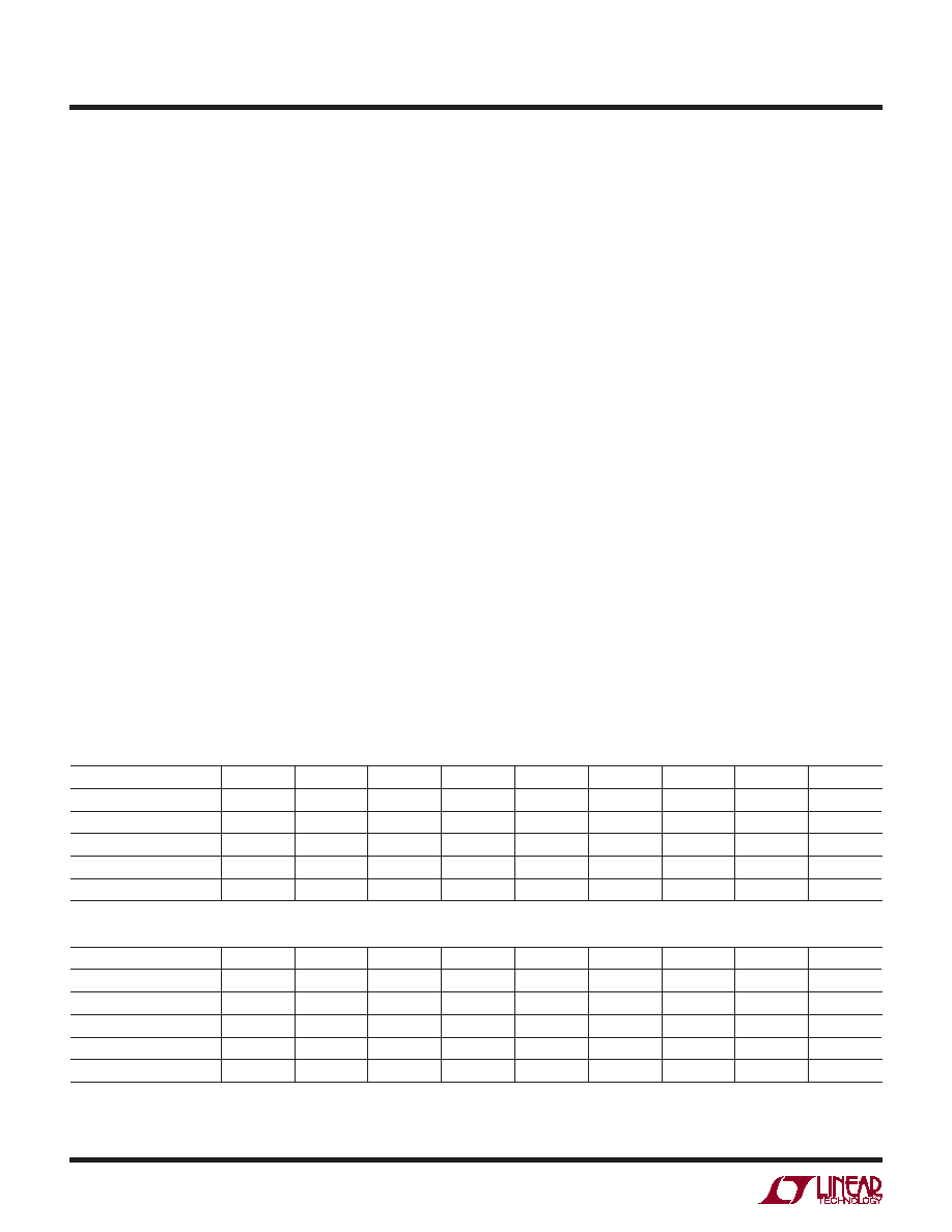
Table 5a. Performance vs Gain in Normal Speed Mode (VCC = 5V, VREF = 5V)
GAIN
1
4
8
16
32
64
128
256
UNIT
Input Span
±2.5
±0.625
±0.312
±0.156
±78m
±39m
±19.5m
±9.76m
V
LSB
38.1
9.54
4.77
2.38
1.19
0.596
0.298
0.149
V
Noise Free Resolution*
65536
32768
16384
Counts
Gain Error
5
8
ppm of FS
Offset Error
0.5
V
Table 5b. Performance vs Gain in 2x Speed Mode (VCC = 5V, VREF = 5V)
GAIN
1
2
4
8
16
32
64
128
UNIT
Input Span
±2.5
±1.25
±0.625
±0.312
±0.156
±78m
±39m
±19.5m
V
LSB
38.1
19.1
9.54
4.77
2.38
1.19
0.596
0.298
V
Noise Free Resolution*
65536
45875
22937
Counts
Gain Error
5
ppm of FS
Offset Error
200
V
*The resolution in counts is calculated as the FS divided by LSB or the RMS noise value, whichever is larger.
发布紧急采购,3分钟左右您将得到回复。
相关PDF资料
LTC2496IUHF#TRPBF
IC ADC 16BIT DELTA SIG 38-QFN
LTC2498IUHF#TRPBF
IC ADC 24BIT 16CH 38-QFN
LTC2600IUFD#PBF
IC DAC OCTAL R-R 16BIT 20-QFN
LTC2602IMS8#TRPBF
IC DAC 16BIT DUAL R-R VOUT 8MSOP
LTC2604IGN-1#TRPBF
IC DAC 16BIT QUAD R-R OUT 16SSOP
LTC2605IGN-1#TRPBF
IC DAC 16BIT OCT I2C 16-SSOP
LTC2606IDD#TRPBF
IC DAC 16BIT I2C V-OUT 10-DFN
LTC2607IDE#TRPBF
IC DAC 16BIT R-R I2C 12-DFN
相关代理商/技术参数
LTC2495CUHF#TRPBF
功能描述:IC ADC 16BIT W/PGA 38-QFN RoHS:是 类别:集成电路 (IC) >> 数据采集 - 模数转换器 系列:- 标准包装:2,500 系列:- 位数:16 采样率(每秒):15 数据接口:MICROWIRE?,串行,SPI? 转换器数目:1 功率耗散(最大):480µW 电压电源:单电源 工作温度:-40°C ~ 85°C 安装类型:表面贴装 封装/外壳:38-WFQFN 裸露焊盘 供应商设备封装:38-QFN(5x7) 包装:带卷 (TR) 输入数目和类型:16 个单端,双极;8 个差分,双极 配用:DC1011A-C-ND - BOARD DELTA SIGMA ADC LTC2494
LTC2495IUHF#PBF
功能描述:IC ADC 16BIT W/PGA 38-QFN RoHS:是 类别:集成电路 (IC) >> 数据采集 - 模数转换器 系列:- 标准包装:1 系列:microPOWER™ 位数:8 采样率(每秒):1M 数据接口:串行,SPI? 转换器数目:1 功率耗散(最大):- 电压电源:模拟和数字 工作温度:-40°C ~ 125°C 安装类型:表面贴装 封装/外壳:24-VFQFN 裸露焊盘 供应商设备封装:24-VQFN 裸露焊盘(4x4) 包装:Digi-Reel® 输入数目和类型:8 个单端,单极 产品目录页面:892 (CN2011-ZH PDF) 其它名称:296-25851-6
LTC2495IUHF#TRPBF
功能描述:IC ADC 16BIT W/PGA 38-QFN RoHS:是 类别:集成电路 (IC) >> 数据采集 - 模数转换器 系列:- 标准包装:1,000 系列:- 位数:16 采样率(每秒):45k 数据接口:串行 转换器数目:2 功率耗散(最大):315mW 电压电源:模拟和数字 工作温度:0°C ~ 70°C 安装类型:表面贴装 封装/外壳:28-SOIC(0.295",7.50mm 宽) 供应商设备封装:28-SOIC W 包装:带卷 (TR) 输入数目和类型:2 个单端,单极
LTC2496CUHF#PBF
功能描述:IC ADC 16BIT DELTA SIG 38-QFN RoHS:是 类别:集成电路 (IC) >> 数据采集 - 模数转换器 系列:- 标准包装:1 系列:microPOWER™ 位数:8 采样率(每秒):1M 数据接口:串行,SPI? 转换器数目:1 功率耗散(最大):- 电压电源:模拟和数字 工作温度:-40°C ~ 125°C 安装类型:表面贴装 封装/外壳:24-VFQFN 裸露焊盘 供应商设备封装:24-VQFN 裸露焊盘(4x4) 包装:Digi-Reel® 输入数目和类型:8 个单端,单极 产品目录页面:892 (CN2011-ZH PDF) 其它名称:296-25851-6
LTC2496CUHF#TRPBF
功能描述:IC ADC 16BIT DELTA SIG 38-QFN RoHS:是 类别:集成电路 (IC) >> 数据采集 - 模数转换器 系列:- 标准包装:2,500 系列:- 位数:16 采样率(每秒):15 数据接口:MICROWIRE?,串行,SPI? 转换器数目:1 功率耗散(最大):480µW 电压电源:单电源 工作温度:-40°C ~ 85°C 安装类型:表面贴装 封装/外壳:38-WFQFN 裸露焊盘 供应商设备封装:38-QFN(5x7) 包装:带卷 (TR) 输入数目和类型:16 个单端,双极;8 个差分,双极 配用:DC1011A-C-ND - BOARD DELTA SIGMA ADC LTC2494
LTC2496IUHF#PBF
功能描述:IC ADC 16BIT DELTA SIG 38-QFN RoHS:是 类别:集成电路 (IC) >> 数据采集 - 模数转换器 系列:- 标准包装:2,500 系列:- 位数:16 采样率(每秒):15 数据接口:MICROWIRE?,串行,SPI? 转换器数目:1 功率耗散(最大):480µW 电压电源:单电源 工作温度:-40°C ~ 85°C 安装类型:表面贴装 封装/外壳:38-WFQFN 裸露焊盘 供应商设备封装:38-QFN(5x7) 包装:带卷 (TR) 输入数目和类型:16 个单端,双极;8 个差分,双极 配用:DC1011A-C-ND - BOARD DELTA SIGMA ADC LTC2494
LTC2496IUHF#TRPBF
功能描述:IC ADC 16BIT DELTA SIG 38-QFN RoHS:是 类别:集成电路 (IC) >> 数据采集 - 模数转换器 系列:- 标准包装:2,500 系列:- 位数:16 采样率(每秒):15 数据接口:MICROWIRE?,串行,SPI? 转换器数目:1 功率耗散(最大):480µW 电压电源:单电源 工作温度:-40°C ~ 85°C 安装类型:表面贴装 封装/外壳:38-WFQFN 裸露焊盘 供应商设备封装:38-QFN(5x7) 包装:带卷 (TR) 输入数目和类型:16 个单端,双极;8 个差分,双极 配用:DC1011A-C-ND - BOARD DELTA SIGMA ADC LTC2494
LTC2497CUHF#PBF
功能描述:IC ADC 16BIT W/PGA 38-QFN RoHS:是 类别:集成电路 (IC) >> 数据采集 - 模数转换器 系列:- 标准包装:1 系列:microPOWER™ 位数:8 采样率(每秒):1M 数据接口:串行,SPI? 转换器数目:1 功率耗散(最大):- 电压电源:模拟和数字 工作温度:-40°C ~ 125°C 安装类型:表面贴装 封装/外壳:24-VFQFN 裸露焊盘 供应商设备封装:24-VQFN 裸露焊盘(4x4) 包装:Digi-Reel® 输入数目和类型:8 个单端,单极 产品目录页面:892 (CN2011-ZH PDF) 其它名称:296-25851-6